As a memory of my last semester, I want to integrate my experience and skills which are gained from previous projects, generally including hardware and firmware.
A good idea to to DIY an audio speaker system that involves circuit design (filter, op-amp, power IC, voltage rectifier, fan etc), PCB layout, mechanical design, and C firmware for volume/bass/treble/balance control. You may also find this design are a little complicated to achieve nice sound quality and customer usability(although not a product), moreover all the circuit design are implemented with a home made PCB.
===============================================================================
I will discuss this design following these chapters:
1. Candidate Drivers
2. Amplifier Design
2.1 Power Supply
2.2 Cooling Fans
2.3 Volume Control
2.4 2-Way Active Crossover
2.5 Power Amplifier IC LM3886
2.6 Heat Toner Transfer PCB Manufacture
2.7 Issues and Debugging Experience
3. Ported Enclosure Design
3.1 Enclosure Design
3.2 Impedance Measurement
4. Test and Evaluation
5. Conclusion
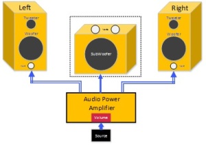
A fully functional 2.0 speaker system, including a power amplifier and two ported enclosures, is built as a DIY project. Fig.1 shows the structure of this 2.0 configuration. The power amplifier features 5 channels *100W output with THD < 0.1%, 2-way active crossover, and adjustable tweeter/woofer level on each channel. Two ported enclosures with woofer and tweeter are designed to provide a good SPL response over a wide frequency range with the active crossover of amplifier. A 2-port subwoofer enclosure is also built to test frequency response under 100Hz.
1.Candidate Drivers
The project was started to build a 2.0 speaker system that could be used in a medium to small room area. So a pair of 50W RMS woofers and a pair of 15W RMS tweeters are selected. These pairs of drivers are carefully selected to match desired maximum RMS output power of amplifier. In this case, the amplifier discussed in next section can drive a 4 Ohm woofer with 100W maximum RMS output with THD<0.1%.
Also, according the SPL of woofer and tweeter, the active crossover is set to 1.8 KHz so that the woofer and tweeter can provide a flat response below 1.8 KHz and above 1.8 KHz respectively.
Please check the detailed specs from the manufactures.
2. Amplifier Design
The section will discuss main functional blocks of this amplifier.
An audio power amplifier with 5 channels and 2-way active crossover on each channel are designed so that it could support either 2.0 or 2.1 configuration. In order to driver the 50W woofers and 15W tweeters, each channel are designed to support 100W RMS output. Active crossovers are designed to tune tweeter and woofer level to get a reasonable SPL response, thus good sound quality.
The main features of this audio power amplifier include:
- 5 channel * 100W RMS output @8Ω.
- Low offset (<1mV) and low noise output.
- Adjustable tweeter and woofer level.
- 2-way active crossover at 1.8 KHz.
- Volume control from -95dB to 31dB.
- Cooling fans with adjustable speed.
Fig.2 shows overview of the audio power amplifier, including 110V main power input, toroid transformer, bridge rectifier, voltage regulators with heat sinks, PCB (volume control, active crossover, and amplifier), arduino, cooling fans. Fig. 2.1 shows the basic structure of each channel.
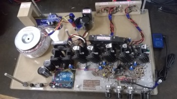 Fig.2 Overview of Audio Power Amplifier
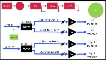
Fig.3 shows a corresponding block structure of this audio power amplifier. Briefly, the red power blocks are to power different functional blocks of the amplifier. Left and Right channels have same structure that audio signal is first controlled by volume block, then crossed and tuned by active crossover network then amplified to drive tweeter/woofer. Orange blocks represent the 5th channel that abstracts signals below 100Hz from both channels then be summed together and amplified to drive the subwoofer. For current 2.0 configuration design, ICs are not populated for 5th channel so that a simplified block structure is shown in Fig.4.
Fig.3 Block Structure Audio Power Amplifier of 2.1 Configuration
Fig.4 Simplified Block Structure Overview of 2.0 Configuration.
2.1 Power Supply:
Toroidal transformer and Bridge rectifier are designed to convert 110V high voltage to rippled DC voltage. Then several pairs of Positive/Negative voltage regulators (LDO) are used for this design, including LM317, 7805, 7905, 7815, 7915, etc, to get clean power supplies.
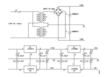 Fig.5 Main Power Supply Schematic
Fig.5 is the schematic of the Power Supply(Note: other pairs of LDOs and necessary capacitors are not shown here). The 100V input is connected to a center tapped toroid transformer through a 10A slow blow fuse. Four 10A rectifier diodes are used as a bridge rectifier. Two 10000uF capacitors are placed at the bridge rectifier output to smooth the final output. Several small capacitors of 1000uF, 47uF and 10uF which are parallel with the 10000uF to further smooth output are not shown here.
The bridge rectifier output of ±38V powers the main power amplifier chip LM3886. A pair of ±15V voltage regulators is used to power operational amplifier of crossover, pre-amp, etc. A pair of ±5V voltage regulators is used to power Arduino, volume control chip, cooling fan, etc.
For stability, heat sinks are sued for each voltage regulator.
Power supply is critical for audio systems. Ideally we need pure DC and quiet power supply. Otherwise, the circuit could easily pick up noise and then amplifier this noise and finally you could hear buzz noise at the drivers even though no audio source are connected. We will talk more about noise in the PCB layout.
2.2 Cooling Fan
Two cooling fans are used to cool down the voltage regulators and amplifier chips since all the chips can get super hot under high volume working condition.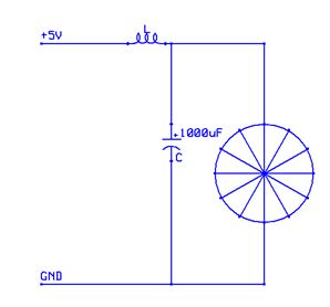 Fan is very noise for both audience and circuit. Two quiet fans used for laptop are selected. To kill the noise that is brought to circuit, a Ferrum core inductor and a 1000uF capacitor are placed as show in Fig.6.
2.3 Volume Control
We can actually use R, C to build complicated circuit for volume/bass/treble/balance control, but we may be concerned with circuit matching, stability thus sound quality. In this design, I designed a active crossover so that we can separately adjust woofer and tweeter volume level, so bass/treble/balance are actually not necessary here. Then what I need is just a volume control function.
A precision resistor-network chip (PGA2310) is used to adjust the volume. Volume gain can be set from -95dB to 31dB by sending data from Arduino to its SPI port to change input and feedback resistor values as shown in Fig.7.
Fig.7 Block structure of Volume Control IC
This design with precision volume control chip has an advantage over dual potentiometer which has two potentiometers that are not ideally equal to each other so that balance problem will exist.
2.4 2-Way Active Crossover
 Fig.8 block structure of 2-Way active crossover
 Fig.9 Comparison of the magnitude response of 2 pole Butterworth and Linkwitz-Riley crossover filters
Figure 8 represents the active crossover structure on both left and right channels. The active crossover network is to split audio signal into low and high frequencies to drive woofer and tweeter respectively. A 2-way 4th order Linkwitz-Riley active crossover by 2 cascading Butterworth filters is implemented for each channel.
Fig.9 shows the comparison of the magnitude response of 2 pole Butterworth and Linkwitz-Riley crossovers. The summed output of the Butterworth filter has a +3dB peak at the crossover frequency while the Linkwitz-Riley has a flat summed output.
A time delay block is implemented to compensate path difference between tweeter and woofer shown in Fig.10. Since the audio source point of woofer is a little behind tweeter, there will be phase difference if without this time block.
Potentiometers are placed to adjust the output level for tweeter and woofer to get a flat output even though tweeter and woofer have different SPL, power, etc.
2.5 Power Amplifier IC LM3886
 Fig.11 LM3886 Schematic Design
Fig.11 shows the basic schematic of the LM3886. The core power amplifier IC is LM3886 which is class AB amplifier and features high output power with low THD. Each LM3886 of 5 channels is powered by ±38V so that the maximum RMS power to 8 Ohm drivers can be 100W with THD < 0.1%.
The reference design can be found from LM3886 datasheet so that details will not be covered here, either the feedback L,C values or the input coupling C. What’s different from recommended schematic is that a 20K resistor is placed at input as a pull-down resistor which will make sure the input of LM3886 is grounded when there is no signal from audio source so no noise will appear at output ideally.
2.6 PCB Layout Design and Heat Toner Transfer Manufacture
PCB layout should be carefully designed so that no undesired noise will exist at output. The main difficulty is the Ground design. Star ground is preferred which is typical design for audio layout.
Heat toner transfer is used to make a 6inch*9inch double layer PCB in lab for low cost and flexible layout. Main steps include:
Design PCB Layout—-Print PCB Layout to glossy paper—-Transfer toner to copper board—-Etch board.
3 Ported Enclosure Design and Measurement
3.1 Enclosure Dimensions
The ported enclosures are designed to get a desired SPL response. Enclosure dimensions and port parameters are calculated according vented-box alignment chart provided in class handouts.
Volume of Tweeter/Woofer enclosure is:
0.65 cu.ft (18.5Ltrs) with a port of D=2″ (5cm), L = 5″ (13cm).
A two-port subwoofer enclosure with volume :of 3.23 cu.ft (91.5Ltrs) is also designed but for test purpose only.
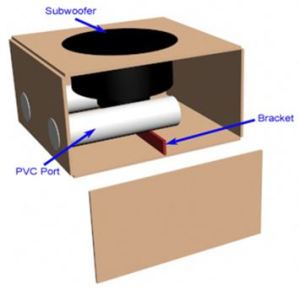
Fig.13 shows the 3D view of these enclosures. Brackets are placed at several key locations. Fiberglass are placed at back, left and bottom at inside surfaces to absorb undesired waves. Caulk is used to seal box.
Fig.15 is the impedance measurement of woofer enclosure with Zobel network. The resonant frequency of the woofer is around 28Hz. Two humps are measured around the resonant frequency that is the effect of the port. Flat impedance over a wide frequency is measured. Overall, this enclosure design meets the requirements.

